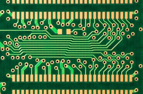
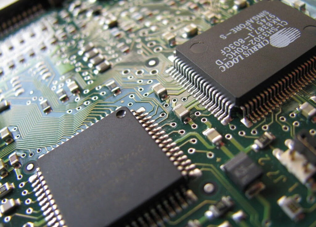
At first glance, PCB (printed circuit board) manufacturing may look complicated due to its intricate structure having conductive elements(pads, traces, and planes) and components. This system provides mechanical support to electronic parts and links them electrically. Thus, it is the main ingredient of modern electronic recipes.
When we talk about the science behind this miniatured network, it is the physics and overall production work involved. Throughout this article, we will examine the core conceptual process of making a circuit board, from bare boards to complete assembly.
It all begins with an appropriate PCB Design
PCB manufacturing process kickstarts with making a conceptual diagram on paper. Using CAD software, this image is transformed into a logical depiction of an electrical circuit, popularly known as Schematics. Schematics consists of electrical symbols, connections, Bill of Materials (BOM), and other parameters. Designers analyze these aspects and prepare a stack-up, a layer-by-layer arrangement of building boards. Finally, a PCB layout consisting of design rule checking (DRC), Component placement, routing, drawings, and other fabrication details are created.
Manufacturer analyzes design files
Designers send all the necessary files, such as BOM, Gerbers, ODB++, etc., to the manufacturer. The manufacturer checks the feasibility of these files by performing design for manufacturing (DFM) checks. DFM is crucial to visualize practical aspects of boards from their theoretical designs. If a violation occurs, the designer will be notified and asked to modify the files.
Later, the CAM software generates output files for different fabrication departments. It includes solder masks, imaging layers, stack-up planning, netlist, etc.
Making a layer-by-layer sandwich (PCB)
As we know, semiconductor manufacturing involves multiple steps, so as PCB manufacturing. The step-by-step approach is briefly mentioned below:
- Printing of circuit images using laser-direct imaging (LDI) or conventional plotting
- Etching to remove unwanted material from the board
- Punching of layers using an optical punch for an accurate layer alignment
- Oxide coating to prevent corrosion and oxidation
- Lamination to join prepreg, copper foils, and inner core together. After lamination, the board is treated through hot and cold pressing to achieve good bondability. This is the process of stack-up preparation.
- Drilling to make holes (for leaded parts) and vias (for leadless components).
- Copper plating to achieve conductivity in holes or hole barrels.
- Tin plating to prevent corrosion of surface features (holes, pads, etc.)
- Final etching and tin stripping are performed.
- Application of solder mask (green appearance).
- Applying a proper surface finish (HASL, OSP, Lead-free HASL, ENIG, Hard gold, immersion silver, etc.). The surface finish increases the shelf life of the board, protects it from environmental conditions, and makes the board surface ideal for soldering.
- Silkscreen printing using manual screen printing and direct legend printing.
- Checking the fundamental electrical properties of the board using an electrical test, popularly called E-test. Two methods are available for executing this test: the flying probe and the bed of nails tester.
This is how PCB manufacturing takes place.
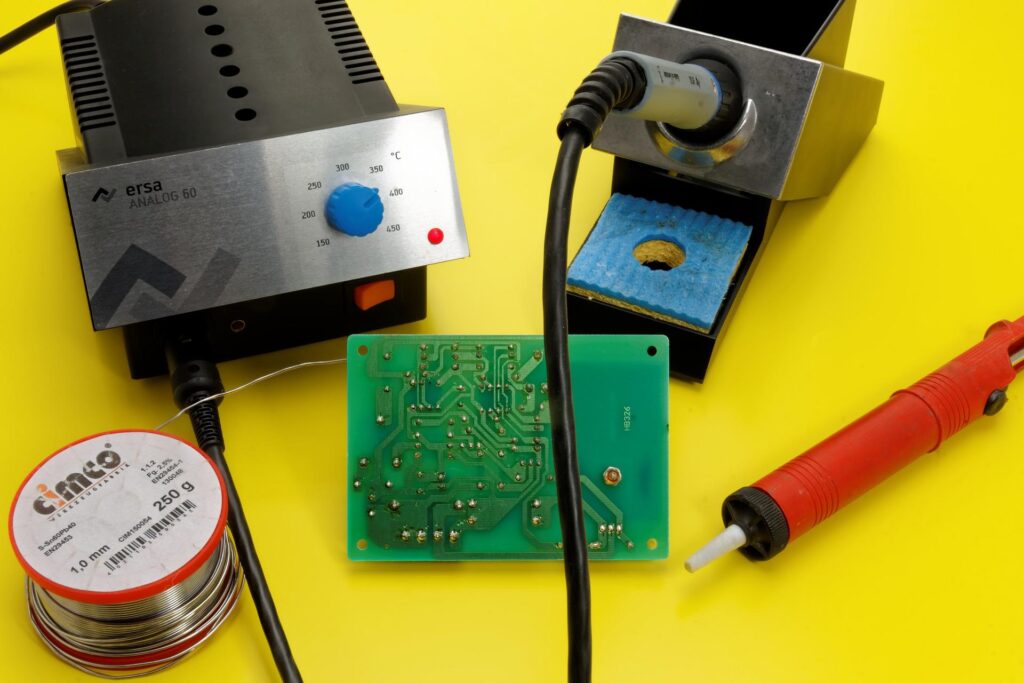
Next, Soldering comes into the picture
Soldering is the backbone of PCB assembly. It is the process of attaching components to the board using solder. This process should achieve proper wettability for the solder to flow without obstruction. This is achieved using soldering flux, which removes oxides and prevents reoxidation. Rosin is the widely used flux.
Three methods are available depending on the complexity and miniaturization of boards. Here is a brief explanation:
- Manual soldering/Hand soldering: This is a preferred way for a board that has a few components (mostly leaded). A flux, adequate heat, and perfect application of solder will result in reliable bonds between parts and the board’s surface.
- Wave soldering: This type is suitable for soldering multiple components quickly. After inserting the parts in holes, the board is placed on a conveyor. This moves the board across a liquid solder pot. In this process, solder is pumped via a chimney and developed into piles along the PCB’s bottom.
- Reflow: This process is ideal when you have a lot of SMDs. This technique requires an application of a solder paste through the stencil. This is done with a solder paste printing machine. Next, the board passes through automatic pick-and-place machines where the parts are placed at the appropriate locations. Then, the whole assembly goes to the reflow oven, where the solder paste melts and sticks components to the surface. This creates enduring solder joints.
Assembling PCBs is a science.
The assembled board has to go through inspections
Now, these boards should be checked for any flaws or defects. Primarily, three inspection checks are executed:
- Manual/visual inspection: This is the easiest way to spot common errors with the naked eye or magnifying glass. This method typically inspects:
- Board dimensions
- Surface quality
- Condition of solder joints
- Position of holes and vias
- Aesthetics
- Automated optical inspection (AOI): This inspection is done during each stage of PCB manufacturing. This method captures images and compares them with the existing standard. Here, proper illumination, a machine vision camera, and processing software are crucial.
- X-ray inspection: This method finds hidden defects in the BGAs (ball grid array) and ICs (integrated circuit). It determines internal geometries, big voids, cracks, and structural compositions. Additionally, it checks for soldering and component defects.
- Functional test: This test qualifies PCBs as pass or fail. This recognizes factors affecting the reliability of the finished boards. Below are the attributes that are checked during this stage:
- Signal integrity
- Power integrity
- Incorrect voltage
- The overall functionality of the board
When the board qualifies for this test, only then is it ready for packaging and shipment.
Finally, finished PCBs are packaged and shipped
This might seem to be the least important aspect of all. But in reality, it is the last item carrying a heavy weight. An ideal packaging protects the board from mechanical damages, environmental hazards, mishandling, and electrostatic shocks. Consider the complexity of your board and choose the packaging accordingly.
- Bubble bag: This is the common packaging required for bare boards.
- ESD packages: These are silver plastic bags suitable for ESD-sensitive boards.
- Vacuum-sealed wraps: Moisture-sensitive boards or components prefer this type of packaging.
- Pink-poly wraps: This plastic wrap is essential for protection against shocks that usually appear during packing and unpacking a lot of boards.
It is the responsibility of every manufacturer to deliver these boards carefully in a quick turnaround time. In addition, the documentation package must accompany the delivery.
Final thoughts
The overall content is not a complete guide to PCB manufacturing but rather a glimpse. Here, manufacturing is defined as a whole process that begins with product conception and ends with the delivery of the final product. Each step has its significance and different parameters or bars to accomplish the desired output. There are many vital parts of PCBs, such as gold fingers, side platings, RoHS compliance, array panelizations, etc., that vary depending on the application.
PCBs are available in different types like flex, rigid, HDI, single-sided, double-sided, and multilayer boards. Distinct sectors choose these types as per classes (class 1, class 2, and class 3) and industry-specific regulations. Demand for PCBs is booming due to recent trends like connected cars, touchscreen technology, underwater monitoring, healthcare, and Cubesats.
If you would like a detailed explanation about any topic mentioned above, please write to us. We would be happy to serve you.

tadalafil https://canadianpharmaceuticalsonline.home.blog/
You explained that exceptionally well.
Thank you, keep reading!
[…] is similar to photolithography or laser direct imaging used in PCB manufacturing. Lasers along with the UV light harden the resin and print the image on a substrate […]
[…] Read more, a journey into the world of PCB manufacturing. […]
[…] our article on 6 easy steps to remember in the world of PCB manufacturing to learn about miniaturized PCB […]
PCB manufacturing can indeed be complex, but you’ve broken it down into six easy-to-understand steps. Starting with the PCB design process and moving through manufacturing, soldering, inspections, and packaging, you’ve covered the entire journey of creating a circuit board. The explanations of different techniques like manual soldering, wave soldering, and reflow were particularly helpful. It’s also good to see the emphasis on inspections and functional tests to ensure quality. Overall, this article provides a concise overview of PCB manufacturing, and I appreciate the offer to provide more detailed explanations if needed. Keep up the good work!
Thank you so much! Keep reading!